
PCB Manufacturing Process: 12 Steps from CAD to Finished Board
PCB manufacturing is a 12-step wet-photographic process that turns a CAD design into a copper-clad, drilled, plated, etched, masked and finished circuit board. The steps are: CAM and tooling prep, substrate cutting, multilayer lamination, mechanical drilling, electroless copper deposition, PTH plating, photoresist imaging, pattern plating, alkaline or acidic etching, solder-mask coating, surface finish (HASL/ENIG/OSP/Immersion), CNC profiling and electrical test. A commercial double-side line needs 25-35 machines; a multilayer line adds lamination and inner-layer processing for 40-55 machines.
A printed circuit board (PCB) is the mechanical and electrical backbone of every electronic product, from a 4-layer smartphone mainboard to a single-side LED light strip. Despite very different end-uses, almost every PCB in the world is built by the same sequence of unit operations — drilling, plating, imaging, etching — arranged in different ways depending on layer count, panel size and required tolerance. This guide walks through that sequence, the materials you choose between, and what a complete wet-process line costs to build and run.
Key Takeaways
- PCB manufacturing is a 12-step wet-photographic process, not one machine.
- Substrate choice (FR4, high-Tg FR4, polyimide, aluminum, Rogers) sets the temperature and chemical budget.
- Single-side, double-side and multilayer boards use the same unit operations, just more of them.
- Alkaline ammonia etching is the modern choice for fine lines; cupric chloride for outer layers and high-volume lines.
- A 31-machine double-side line for 100 m²/month starts around USD 420,000.
What Is a PCB?
A PCB is a flat laminate of an electrically insulating substrate with copper foil bonded to one or both sides. The copper is patterned into traces, pads and planes that connect the components soldered onto the board. Drill holes — either plain through-holes or plated through-holes (PTH) — carry signals between layers. A solder mask covers most of the copper to prevent solder bridges, and a surface finish on the exposed pads protects the copper from oxidation and ensures a solderable or wire-bondable surface.
The simplest board, a single-side PCB, has copper on one side only and no PTH. It is used in low-cost consumer and lighting products. A double-side PCB has copper on both sides connected by PTH and covers the majority of commercial electronics. Multilayer PCBs add two or more inner copper layers laminated between sheets of partially-cured epoxy (prepreg) for high-density designs such as smartphones, networking switches and medical imaging hardware.
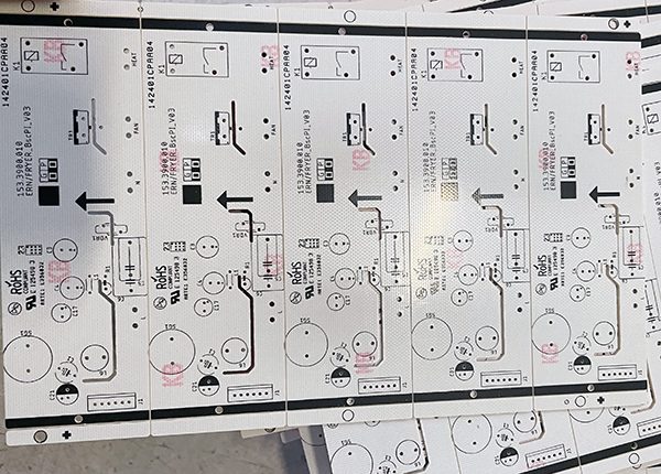
The 12-Step PCB Manufacturing Workflow
Each step is its own wet-process unit operation and uses dedicated machines. Skipping a step or combining steps is possible for prototypes, but commercial quality requires each step to be properly controlled. The table below summarizes the sequence, the chemistry or mechanics involved, and the machine that runs it.
| # | Step | Process | Machine |
|---|---|---|---|
| 1 | CAM & tooling | Gerber check, panelization, drill file | CAM software |
| 2 | Cutting | Shear or V-cut substrate to working panel | PCB board cutting machine |
| 3 | Lamination | Laminate dry-film photoresist onto copper surface under heat & pressure | Dry film photoresist laminator |
| 4 | Drilling | Mechanical or laser drill through-holes & vias | CNC PCB drilling machine |
| 5 | Deburr & brush | Remove drill smear and edge burrs | PCB brushing & deburring machine |
| 6 | Electroless Cu | Deposit thin conductive copper on hole walls | Electroless copper line |
| 7 | Imaging | Laminate photoresist, expose, develop | Dry-film laminator + exposure + developer |
| 8 | Pattern plating | Electroplate copper + tin-lead on exposed pads | PCB electroplating line |
| 9 | Etching | Spray alkaline or cupric chloride to remove background copper | PCB etching machine |
| 10 | Solder mask | Coat, expose & cure epoxy mask | Solder mask coating + exposure line |
| 11 | Surface finish | Apply HASL / ENIG / OSP / Imm. Sn-Ag | Surface finish line |
| 12 | Profiling & test | CNC route panel, electrical test, final inspection | CNC routing machine + flying probe tester |
For multilayer boards, the sequence repeats for each inner layer: cut, image, etch, inspect, then laminate into the stack before outer-layer drilling and plating begin. A 4-layer board therefore has three imaging and two etching cycles before the outer layers are processed.
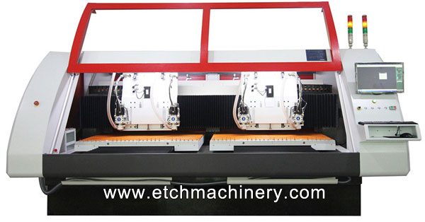
Why Etching Is the Step That Defines the Line
Etching is where the actual circuit pattern is created — everything before imaging defines where the resist will protect the copper, and everything after plating just preserves what etching leaves behind. Etch uniformity, etch factor, and side-cut determine minimum trace width and spacing. A line that swings its etch chemistry temperature by more than ±2 °C will see ±15% trace-width variation across the panel, which is the single most common cause of scrap in commercial PCB production.
Substrate Comparison
The substrate sets the thermal, mechanical and chemical budget for the entire line. The wrong substrate choice can mean re-tooling the lamination press, switching to lead-free HASL chemistry, or qualifying a new electroless copper bath. The table below covers the five substrates used in >95% of commercial PCBs.
| Substrate | Tg (°C) | Dk @ 1 MHz | Cost Index | Typical Use |
|---|---|---|---|---|
| FR-4 (standard) | 130-140 | 4.3-4.6 | 1.0× | Consumer electronics, single/double-side |
| High-Tg FR-4 | 150-180 | 4.2-4.5 | 1.3× | Lead-free assembly, multilayer, automotive |
| CEM-1 / CEM-3 | 110-130 | 4.5-5.0 | 0.85× | Single-side consumer, LED lighting |
| Polyimide | 260+ | 3.4-3.8 | 4-6× | Flexible PCBs, aerospace, high-temp |
| Aluminum (IMS) | 130-150 | — | 2-3× | LED lighting, power modules |
| Rogers / PTFE | 280+ | 2.2-3.5 | 8-15× | RF, microwave, 5G, radar |
Standard FR-4 covers >80% of commercial boards. High-Tg FR-4 is required whenever the board will pass a lead-free reflow oven at 260 °C peak — the higher Tg prevents delamination and pad lifting. Polyimide is used for flex and rigid-flex; aluminum (IMS, insulated metal substrate) is for LED boards that need direct thermal conduction to the LED junction.
Single-Side vs Double-Side vs Multilayer
The layer count drives the line complexity. A single-side line can be as small as 8 machines and run profitably at 50 m²/month. A double-side line needs 25-35 machines and 100-200 m²/month to break even. A multilayer line adds inner-layer imaging and lamination and typically starts at 40 machines and 200+ m²/month.
| Parameter | Single-Side | Double-Side | Multilayer (4-layer) |
|---|---|---|---|
| Machines in line | 8-15 | 25-35 | 40-55 |
| PTH plating step | Not required | Required | Required |
| Inner-layer imaging | No | No | 2 additional cycles |
| Lamination cycles | 0 | 0 | 1 |
| Min trace/space (typical) | 8/8 mil | 5/5 mil | 3/3 mil |
| Capital cost (USD) | 150-280 K | 350-500 K | 700 K-1.2 M |
| Typical end product | LED strip, remote control | Consumer electronics, power supply | Smartphone, router, ECU |
For a first-line entry into PCB manufacturing, double-side with PTH is the sweet spot: 80% of commercial demand, mid-tier capital cost, and room to scale up to 4-layer without throwing away existing equipment.
Etching Process Deep-Dive
Two etchant chemistries dominate modern PCB manufacturing. Both dissolve copper, but they behave differently and are used in different parts of the line.
Alkaline Ammonia Etching
Alkaline ammonia (Cu(NH34 2+) is the modern workhorse for inner-layer fine-line etching. It is fast, gives a near-vertical etch factor, and does not attack dry-film photoresist. The chemistry is regenerable: a closed-loop system adds air, ammonia and water to bring the copper concentration back to the operating window without dumping spent solution.
- Etch rate: 30-50 µm/min on exposed copper
- Etch factor: 2.5-4.0 (vertical vs lateral)
- Best for: inner layers, fine-line outer layers, high-density designs
- Drawback: ammonia fumes require scrubbing; not ideal for thin 0.5 oz copper
Acidic Cupric Chloride Etching
Cupric chloride (CuCl2) is the classic PCB etchant and remains the first choice for high-volume outer layers. It etches 1 oz copper in about 60 seconds in a conveyor spray machine, is easily regenerated with chlorine or peroxide, and tolerates wide variation in copper loading.
- Etch rate: 35-55 µm/min
- Etch factor: 2.0-3.0
- Best for: outer layers, high-volume production, 1-2 oz copper
- Drawback: attacks dry-film photoresist if over-sprayed; side-cut higher than alkaline

Surface Finish Comparison
Surface finish protects the exposed copper pads from oxidation and gives a solderable or wire-bondable surface. The four finishes below cover >95% of commercial use.
| Finish | Thickness | Shelf Life | Cost Index | Best For |
|---|---|---|---|---|
| HASL (SnPb) | 1-40 µm | 12 months | 1.0× | Through-hole, low-cost consumer |
| Lead-free HASL (SnAgCu) | 1-40 µm | 12 months | 1.1× | Lead-free assembly, through-hole |
| ENIG (Ni/Au) | 3-6 µm Ni + 0.05-0.1 µm Au | 12 months | 1.6× | Fine-pitch BGA, aluminum wire bond |
| OSP (organic) | 0.2-0.5 µm | 3-6 months | 0.7× | Lead-free SMT, short supply chain |
| Immersion Tin | 0.8-1.2 µm | 6 months | 1.3× | Press-fit, backplanes |
| Immersion Silver | 0.1-0.3 µm | 6 months | 1.4× | Aluminum wire bond, RF |
For a new line, lead-free HASL and OSP give the best cost-vs-flexibility balance. ENIG adds about USD 30,000-50,000 of equipment for a 100 m²/month line but unlocks fine-pitch BGA and wire-bond work that HASL cannot do.
5-Year TCO Model
A PCB wet-process line has four cost drivers: equipment depreciation, chemistry, labor and energy. The table below models a 31-machine double-side line running 100 m²/month, 24 hours / day, 25 days a month.
| Cost Driver | Year 1 | Year 2 | Year 3 | Year 4 | Year 5 | 5-Year Total |
|---|---|---|---|---|---|---|
| Equipment depreciation | 84 K | 84 K | 84 K | 84 K | 84 K | 420 K |
| Chemistry (Cu, SnPb, etchant) | 72 K | 78 K | 82 K | 88 K | 92 K | 412 K |
| Labor (4-shift, 8 ops) | 96 K | 102 K | 108 K | 114 K | 120 K | 540 K |
| Energy (spray pumps, heating) | 54 K | 58 K | 62 K | 65 K | 68 K | 307 K |
| Maintenance & spares | 18 K | 22 K | 26 K | 30 K | 34 K | 130 K |
| Waste treatment | 14 K | 15 K | 16 K | 17 K | 18 K | 80 K |
| Annual total | 338 K | 359 K | 378 K | 398 K | 416 K | 1.89 M |
| USD per m² | 282 | 299 | 315 | 332 | 347 | 315 avg |
The dominant cost is labor (29%) and chemistry (22%). A line in a low-wage region or with high automation can drive USD/m² down to USD 220; a Western European or North American line typically runs USD 350-420/m² before margin.
Industry Applications
PCBs built on a Golden Eagle line serve every segment of the electronics industry. The five products below are the highest-volume end-uses for a 100 m²/month line.

LED Lighting Strips
Single-side aluminum-substrate (IMS) PCBs that draw heat directly out of the LED junction. Built on a 8-machine single-side line running CEM or FR-4 substrate.
Consumer Electronics
Double-side FR-4 with ENIG finish for smartphones, routers, set-top boxes, remote controls, and small home appliances. The workhorse application for 31-machine lines.

Automotive ECUs
High-Tg FR-4 multilayer PCBs (4-6 layers) with lead-free HASL or ENIG, qualified to AEC-Q100. Tolerates 150 °C ambient under-hood operation.

Industrial & IoT
4-layer to 8-layer PCBs for industrial controllers, PLCs, IoT gateways, and sensor hubs. Often Rogers or hybrid stack-up for RF performance.

Medical Devices
High-density multilayer boards for patient monitors, ultrasound front-ends, and implantables. Biocompatible surface finishes, tight ±10% impedance control.
Golden Eagle Equipment Lineup
Beijing Golden Eagle supplies complete wet-process PCB lines covering every step in the 12-step workflow. The lineup below is the 25-35 machine scope most commonly quoted for a 100 m²/month double-side line.
PCB Production Equipment
Wet-process machines used in the 12-step PCB manufacturing workflow:
-
 Cutting
PCB Board Cutting Machine
GE-C650 series, shear & V-cut
-
Drilling
CNC PCB Drilling Machine
GE-D4 series, 200 krpm
-
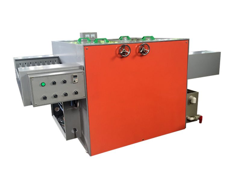 Deburr
PCB Brushing & Deburring Machine
GE-BD650, wet + dry brush
-
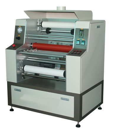 Lamination
Dry Film Photoresist Laminator
GE-DRL series, 400-650 mm
-
 Imaging
LED UV Exposure Machine
GE-LED series, 365-405 nm
-
 Developing
PCB Developing Machine
GE-D650W sodium carbonate
-
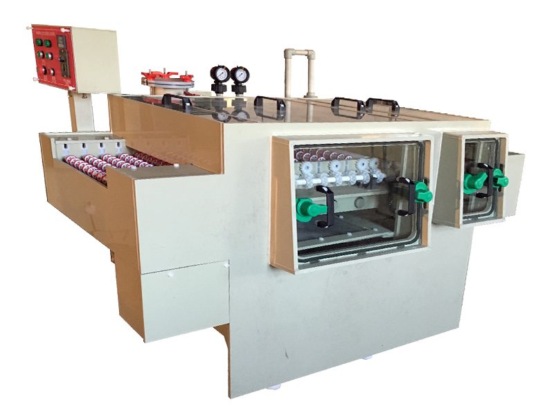
Etching
PCB Etching Machine
GE-650 alkaline or CuCl2
-
 Solder Mask
 Coating Machine
GE-SM650 double-side
-
 Curing
PCB UV Curing Machine
GE-UV365C, 365 nm UV-LED
-
 Surface Finish
ENIG Plating Machine
GE-ENIG series, 3-6 µm Ni + Au
-
 Finishing
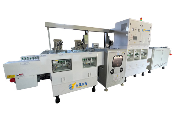
PCB Washing & Drying Machine
GE-WD650 final rinse
-
 Test
PCB Flying Probe Tester
GE-FPT4, 4-head high-speed
Frequently Asked Questions
How many steps are there in PCB manufacturing?
Twelve production steps from CAD/Gerber input to finished panel: cutting, lamination, drilling, electroless copper, PTH, imaging, plating, etching, solder mask, surface finish, profiling and electrical test. Prototype and high-volume lines use the same sequence but at different scales.
What is the difference between single-side, double-side and multilayer PCB?
Single-side has copper on one side only, used in low-cost consumer and lighting products. Double-side has copper on both sides connected by plated through-holes (PTH) and covers 80%+ of commercial electronics. Multilayer (4, 6, 8+ layers) adds inner copper layers laminated between prepreg for high-density designs such as smartphones and networking gear.
Which etching chemistry is used for PCBs?
Two main etchants are used industrially: alkaline ammonia (Cu(NH3)4 2+) for inner layers and fine lines, and acidic cupric chloride (CuCl2) for outer layers and high-volume lines. Both are sprayed under pressure in a conveyor etching machine at 45-55 °C.
What surface finish should I choose for my PCB?
HASL (SnPb or lead-free) is cheapest and most reworkable. ENIG (Ni/Au) gives flat pads for fine-pitch BGAs and aluminum wire bonding. OSP is lead-free and cheap but limited shelf life. Immersion tin and immersion silver are niche choices for specific reliability or bonding requirements.
How much does a complete PCB production line cost?
A 25-machine single-side line with 100 m²/month capacity starts around USD 280,000. A 31-machine double-side line with the same capacity is around USD 420,000. A 50-machine multilayer line with 4-layer capability is USD 850,000 and up. Etchant regeneration, waste treatment and cleanroom add another 15-25%.
Can Golden Eagle supply the full line?
Yes. Beijing Golden Eagle supplies 25-50 machine wet-process lines covering cutting, drilling, electroless copper, imaging, plating, etching, solder mask, surface finish, profiling and AOI. Lines ship in 90-150 days with on-site installation, training and lifetime remote support.