
PCB Production Guide
A complete walkthrough of the 31-machine double-side PCB production line, from material prep to final pack-out. Stage-by-stage machine selection, throughput calculation, panel size, and budget for a 100 m²/month shop.
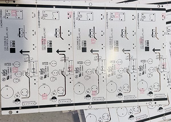
A double-side printed circuit board is the workhorse of nearly every consumer, industrial, and automotive electronic product on the market. Making one requires nine sequential process stages — cutting, drilling, electroless copper, imaging, plating, etching, solder mask, surface finish, profiling — and a typical commercial line uses 25 to 35 individual machines to do the job. This guide walks through each stage, the machines you need, and how to size a line for your target monthly output.
A double-side PCB has copper traces on both the top and bottom surfaces, plated through-holes (PTH) connecting the two sides, and usually a solder mask and surface finish. It is the minimum complexity you need for any product with more than about 8–10 components or any kind of through-hole part. Most double-side boards are made on 1.0–1.6 mm FR-4 substrate, in panel sizes from 200×250 mm (small batch) up to 610×460 mm (mass production). For higher-density work, multilayer PCBs (4, 6, 8 layers) start from the same process plus extra lamination steps.
Each stage is its own mini-process and uses dedicated machines. Skipping a stage or combining stages is possible for prototypes, but commercial quality requires each step to be properly controlled.
FR-4 sheets arrive in standard 1.0×1.0 m or 1.2×1.0 m panels. The first machine is a PCB board cutting machine (V-cut or shear) that breaks them down to the working panel size. After cutting, a deburring-brushing machine removes the edge burrs and surface oxidation. For a 1 m²/day shop this stage uses 1 cutting + 1 deburring machine running about 4 hours per shift.

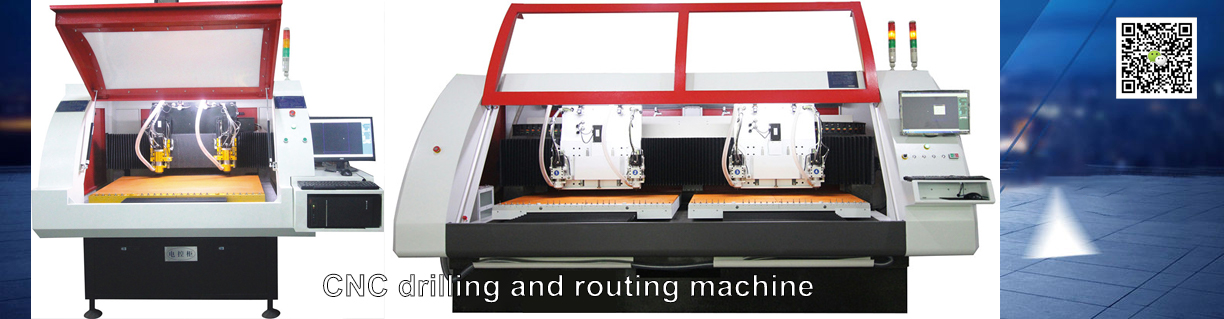
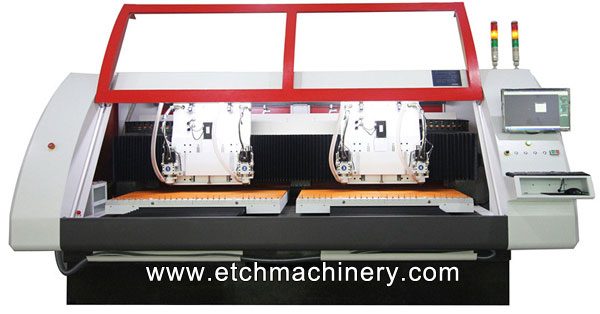
Mechanical drilling with tungsten-carbide bits is still the standard for through-holes above 0.2 mm. A 3-spindle CNC drilling machine handles 35,000–60,000 holes per shift; a 6-spindle machine does 70,000–120,000. For via holes below 0.15 mm a UV or CO2 laser drilling machine is added. Drill entry and exit boards (aluminum or phenolic) protect the panel surface.
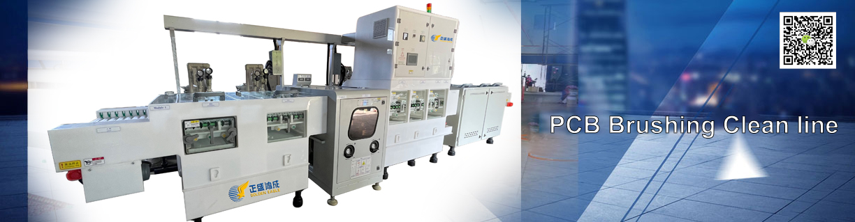
After drilling, the hole walls are non-conductive. The electroless copper line deposits a 0.5–1.0 µm copper layer inside the holes so they can carry current between the two sides. A typical horizontal PTH line includes cleaning, conditioning, micro-etch, predip, activator (Pd/Sn colloid), accelerator, electroless copper, and anti-tarnish. The whole line runs at 2–3 m/min and needs careful solution control.

Dry-film photoresist is laminated onto both sides of the panel in a hot-roll laminator, then exposed through a phototool or directly by an LDI (Laser Direct Imaging) machine. The pattern is then developed in a sodium carbonate spray machine. This stage is the most sensitive for line & space resolution. See our PCB developing machine buying guide for the developing step in detail.


A copper electroplating line adds 20–25 µm of copper into the holes and onto the pattern, then a tin plating layer (~5 µm) acts as an etch resist. Modern lines use horizontal conveyorized cells with rectifier control, solution filtration, and automatic dosing. A typical plating cell is 4–8 m long and operates at 1–3 m/min for the copper stage.


The exposed copper (not protected by tin) is dissolved in an alkaline ammonia or cupric chloride etching machine. The tin is then stripped in a separate line, leaving the circuit pattern. A double-side conveyor etching machine at 2 m/min handles about 30 m²/hour. Etch chemistry, spray pressure, and conveyor speed all directly control line width and undercut.

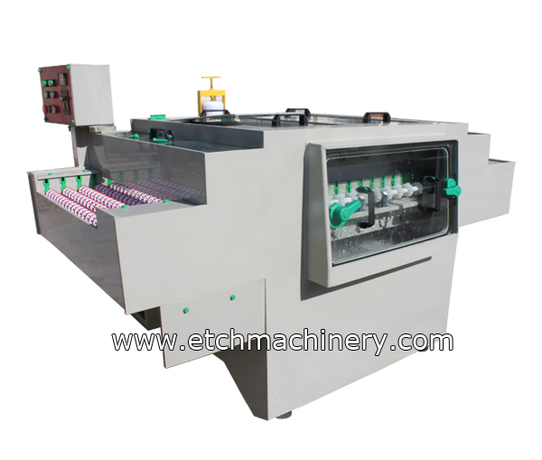
Liquid photoimageable solder mask (LPISM) is screen-printed or curtain-coated onto both sides, pre-baked, exposed through a phototool, developed, and finally UV + thermal cured. This stage uses 4–5 machines: printer, pre-bake oven, exposure machine, developing machine, and UV-curing + thermal-cure oven.
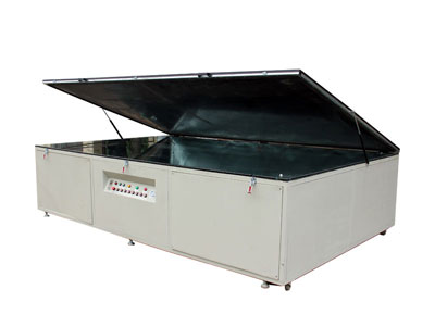
The exposed copper pads need a finish that is solderable and shelf-stable. The four most common finishes are: HASL (hot air solder leveling — lead or lead-free), ENIG (electroless nickel / immersion gold), OSP (organic solderability preservative), and immersion tin or immersion silver. HASL is cheapest; ENIG is best for fine-pitch and wire bonding; OSP is the standard for consumer electronics. Each finish has its own dedicated line.
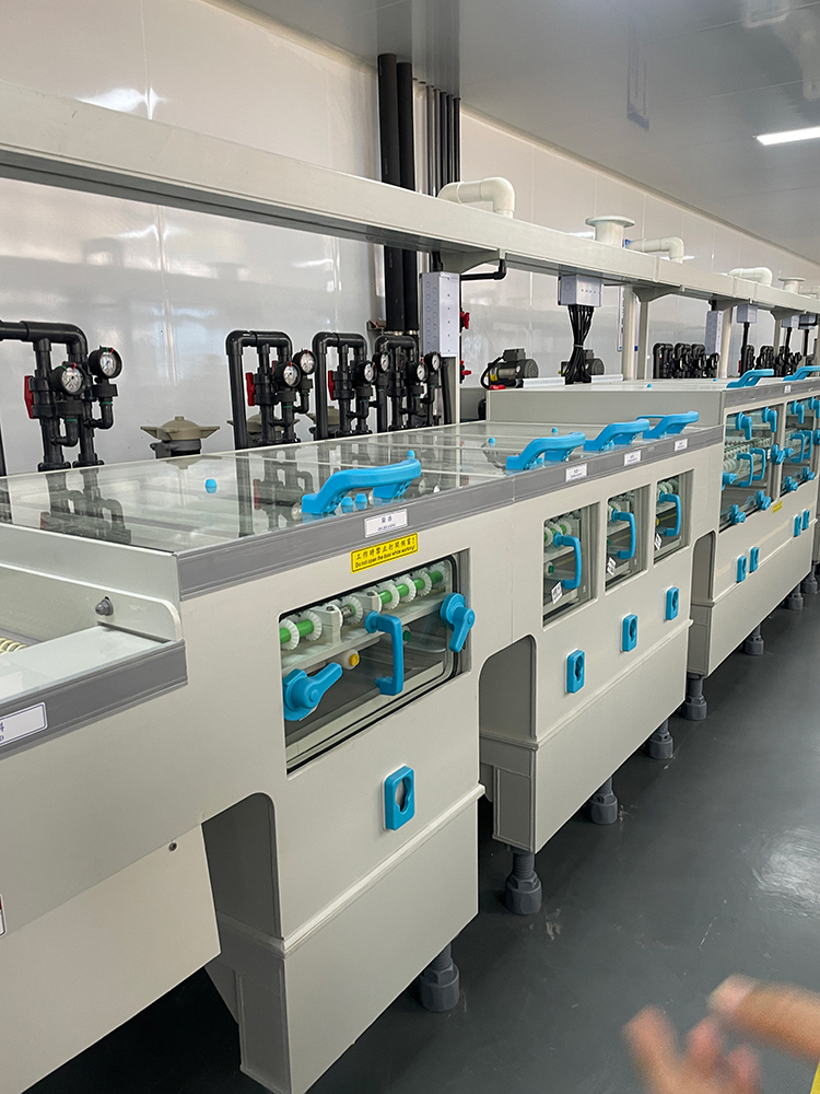
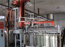
The finished panel is routed into individual boards by a CNC profiling router or V-cut machine. Then electrical test (flying probe or bed-of-nails), AOI (automated optical inspection), final cleaning, and vacuum-pack with desiccant. This stage is 4–6 machines depending on the test coverage.


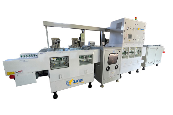
The bottleneck of a PCB line is almost always the imaging + plating + etching section, not the drilling or finishing. For a small-to-medium commercial line targeting 100 m² of finished board per month (about 4,000 m²/year), the typical bottleneck calculation is: assume 25 working days/month × 2 shifts/day × 8 hours/shift = 400 hours/month. 100 m²/month = 0.25 m²/hour average throughput. The etching machine, running at 1–2 m/min on 610 mm wide conveyor, can do 30–60 m²/hour — so the line is comfortably able to hit the target. The bottleneck tends to be yield rather than raw speed once you get past 100 m²/month.
Our standard 31-machine commercial line breaks down as: material prep 3, drilling 2, PTH line 1, imaging 4, plating line 3, etching 2, solder mask 4, surface finish 4, profiling 2, inspection 2, cleaning & pack 2, utilities & auxiliaries 2. Each machine is sized to the bottleneck rate of the line. For full specifications see our 31-machine double-side PCB line product page.
A 31-machine line in a continuous conveyor layout needs about 1,500–2,000 m² of floor space, 8–10 m ceiling height for the exhaust hoods, three-phase 380 V power at 600–800 kVA, and roughly 30–50 m³/day of process water. Wastewater is segregated into copper-bearing, nickel-bearing, lead-bearing, and general rinse streams — see our wastewater treatment guide for compliance details.
A single-side line skips Stages 3 (PTH) and 5 (electroplating) and uses a simpler print-etch-print process. It is significantly cheaper (about 40% of the equipment cost) but only suitable for very simple boards like LED lighting panels or single-side consumer products. For any commercial PCB shop today, a double-side line is the minimum entry point, and a 4-layer multilayer capability is usually added within 2–3 years of operation.